By Jaegwan Shim SEMI, June 25, 2024
With semiconductor materials key enablers of industry growth, experts gathered at SMC Korea to explore the materials market challenges and opportunities ahead.
Advances in semiconductor materials and transistor structures will be crucial for continuous scaling of logic devices, and EUV technology will be essential in driving these innovations, Seong Tae Oh, a Fellow at TEL, said in his keynote address at SMC (Strategic Materials Conference) Korea 2024 in Gyeonggi-do, South Korea in late May. While stochastic noise in EUV lithography can hamper chip performance, he expressed confidence that material innovation will enable the industry to overcome that key challenge.
In his presentation titled Process Technologies for Continuous Scaling of Logic Devices, Oh described a roadmap for the future of semiconductor scaling, noting that the density of logic semiconductors is increasing by 1.74 times every two years. At the same time, SRAM density is rising by 1.49 times. Key factors driving this trend include advancements in materials, transistor structures, and EUV lithography.
Oh predicted that by 2025, 2nm Gate-All-Around (GAA) nanosheet transistors process will be available, by 2029 10-angstrom nodes with CFET transistors will materialize, and by 2033 5-angstrom nodes will emerge with third-generation CFET technology.
He also outlined TEL’s three initiatives for advancing etch technology towards EUV lithography:
- Improving post-lithography variation through repeated deposition and etch processes
- Enhancing mask selectivity by leaving film on resist
- Leveraging collaborations with imec and ASML to develop patterning solutions for the high-NA (numerical aperture) generation

Seong Tae Oh, Fellow at TEL
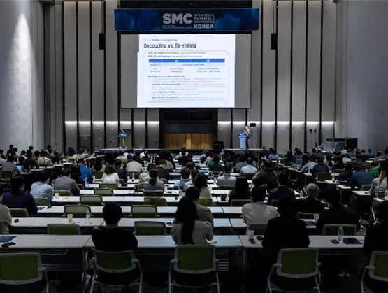
Oh was among 14 renowned visionaries from leading companies in the industry to present under theme Materials Resilience: Navigating Challenges, Embracing Opportunities. Attended by about 300 industry professionals, the 9th annual SMC Korea featured insights not only representatives from semiconductor materials companies but also thought leaders from equipment manufacturers, chipmakers, and research institutes. The event’s goal: Drive toward a holistic approach to addressing industry challenges. The presentations focused on key issues including sustainability and supply chain continuity from an ecosystem-wide perspective.
Following the keynote speech, presenters offered insights on the outlook for the global semiconductor materials market, shifts in the supply chain, and the challenges facing the materials industry.
Dry Resist for Holistic EUV Patterning – Lam Research
In Session 2, themed Advanced Materials, Seongjun Heo, Process Engineering Director of Lam Research, highlighted the following advantages of EUV dry resist technology:
- In combination with ASML’s EUV scanners and Lam’s holistic patterning solutions, EUV dry resist will extend the patterning roadmap (Moore’s Law) for the next decade and beyond.
- The technology offers a high-resolution, high-fidelity, defect-free, and environmentally friendly solution for ≤32nm pitch line/space (L/S) and ≤40nm pitch pillar and contact hole EUV patterning in semiconductor fabrication.

- Addressing critical high-volume manufacturing challenges of advanced logic and DRAM products, dry resist has demonstrated superior dose-to-defectivity for <32nm pitch L/S, making it highly suitable for logic applications.
- EUV dry resist provides ultra-low capillary force during processing, making it ideal for pillar and high aspect ratio patterning.
- The innovation is uniquely suited for future high-NA) EUV patterning, thanks to robust resist thickness scaling while maintaining high etch selectivity and high contrast.

Seongjun Heo, Process Engineering Director at Lam Research
Semiconductor Industry Sustainability Challenges – SK hynix
Speaking during Session 3, on Sustainability, Yongsung Kim, Team Leader at SK hynix, said the annual amount of electronic waste doubled in the past 12 years owing to the march of technological innovation and short lifecycles of electrical equipment.
Of the 62 billion kilogram of e-waste generated in 2022, approximately 50% was metals and 30% plastics, while materials such as glass and minerals accounted for the other 20%, Kim said. Geographically, Kim noted that the level of e-waste collection and recycling varies by region, and that these eco-friendly practices need greater attention by the global chip industry. Today, Europe collects 40% of all cast-off electronic materials, the Americas 30% and Asia 10%.
 For its part, Kim said, SK hynix plans to increase the proportion, based on weight, of recycled materials used in its products to 25% by 2025 and more than 30% by 2030 as the company increases its focus on sustainability under its PRISM (Pursue, Restore, Innovate, Synchronize, Motivate) model. He pointed out that the company will focus on recycling metals such as copper and tin and has developed the industry’s first neon gas recycling technology with TEMC, a domestic manufacturer of specialty gas for the semiconductor sector, to enable a neon recovery rate of 72.7%.

Youngsung Kim, Team Leader at SK hynix
Collaboration – Samsung Electronics and SK hynix
In Session 4, on Collaboration, Ki-Ill Moon, Vice President of SK hynix, underscored the expanding advanced packaging ecosystem driven by emerging computing markets such as AI. He noted that 2.5D packaging – which integrates memory, logic, and other components – is enabling higher chip performance and evolving to address diverse platforms. Moon highlighted the necessity for new, reliable materials that can meet the evolving requirements of these advanced platforms, presenting both challenges and opportunities.
He emphasized that demand for tall pillars in packaging will gradually increase, and that temporary bonding materials are expected to evolve to accommodate various de-bonding forms. He also explained that not only innovation in semiconductor materials but also mutual collaboration among various semiconductor players is the key to developing new technologies for advanced semiconductors.
Sungjun Park, Executive Vice President at Samsung Electronics, addressing the exponential increase of data fueled by digital transformation including the proliferation of smart, connected devices and AI, pointed out that while data volume in 2010 was 2 Zettabytes (ZB), it is projected to reach 181 ZB by 2025 – requiring the development of more advanced chips to process this staggering volume of data.

He highlighted the importance of conventional scaling down, 3D stacking (including advanced packaging), and the introduction of new memory technologies as the chip industry responds to the surge in data generation – and the criticality of the need for innovation of in-fab materials to support these advances.
Park stressed the importance of collaboration and open discussions in spurring innovation in key areas including photoresists (PR) for fine patterning, precursors for selective, conformal deposition, low-temperature processes, CMP slurry without scratch, etchants with higher selectivity, and materials that promote sustainability.
Market Trends – Yole Group and Linx Consulting
Addressing market trends and the outlook for advanced packaging materials Stefan CHITORAGA, a Yole Group Technology and Market Analyst, explained that current high-end performance packaging materials can be categorized by technology into ultra high-density fan-out, 3D NAND, 3D SoC, HBM, co-embedded multi-die interconnect bridge), mold interposer, 3D dimensional stack), Si bridge, 3D DRAM, Foveros, and Si interposer. The advanced packaging materials market, valued at $2.7 billion in 2023, is projected to log a compound annual growth rate (CAGR) of 38% to $18.4 billion by 2029 – a staggering 581% increase.

The largest segment, 3D NAND, valued at $909 million in 2023, is forecast to reach $6.6 billion by 2029, eye-watering growth of 633% fueled primarily by data center networking, high-performance computing, and autonomous vehicles, CHITORAGA said. And while the markets for 3D SoC, mold interposer, and RDL interposer continue to expand, the Si interposer market share for 2D and 3D packaging is anticipated to decline from 84% in 2023 to 44% in 2029.
Presenting on the state of the semiconductor materials market, Mark Thirsk, Managing Director of Linx Consulting, said the market’s current value of $15 billion is projected to double to $30 billion by 2030. With the semiconductor market expected to reach $1 trillion by turn of the new decade, the long-term outlook for semiconductor materials holds great promise. Yet, supply chain challenges pose significant risks for the industry’s growth.
Thirsk pointed to global conflicts that are exposing vulnerabilities in logistics and causing material shortages and heightening uncertainties over the availability of raw materials across the entire supply chain, which, in turn, are driving energy inflation. The shift towards localized production facilities, rather than global ones, may also increase costs in the materials industry.

Mark Thirsk, Managing Director of Linx-consulting